
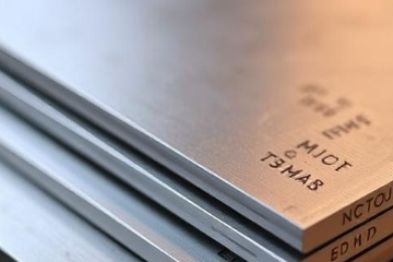


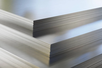


Defining Ultra-High Purity Titanium for Advanced Thin-Film Deposition
Modern microelectronics demand perfection. When we talk about Ultra-High Purity (UHP) Titanium, we aren't just discussing clean metal. We are discussing the backbone of the PVD sputtering process. In a world where transistors are measured in atoms, a single stray oxygen molecule or an uncontrolled grain boundary can ruin an entire wafer batch.
"Ultra-High Purity Titanium Sputtering Targets are specialized metal sources used in Physical Vapor Deposition (PVD) to create thin films of titanium or titanium nitride (TiN) on silicon wafers, characterized by a purity of 99.999% or higher."
At China Titanium Factory, we treat purity as a functional requirement, not a marketing metric. The shift from 4N to 5N and 6N is driven by the shrinking geometry of VLSI circuits. As interconnects get thinner, the margin for error disappears.

The Purity-Performance Matrix: Comparing 5N vs. 6N Titanium Standards
The difference between 5N (99.999%) and 6N (99.9999%) might seem like a rounding error. It isn't. In semiconductor fabrication, that extra "9" represents a tenfold reduction in metallic impurities like Iron (Fe), Copper (Cu), and Sodium (Na). These elements are mobile ions; if they migrate into the silicon, they kill the device performance.
The 100ppm Oxygen Threshold
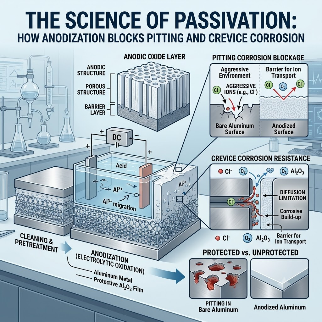
Oxygen is the enemy of conductivity. We've established The 100ppm Purity Principle: To maintain stable sheet resistance in TiN diffusion barriers, the oxygen content in the source target must be strictly controlled below 100ppm. Higher oxygen levels lead to increased "poisoning" of the target surface during reactive sputtering. This results in arc events and macro-particle contamination.
| Metric | 5N (99.999%) | 6N (99.9999%) |
|---|---|---|
| Total Metallic Impurities | < 10 ppm | < 1 ppm |
| Oxygen (O) Content | < 200 ppm | < 100 ppm |
| Primary Application | Standard ICs / LED | Advanced Nodes (<14nm) |
Critical Applications in Semiconductor and VLSI Manufacturing
Why do engineers obsess over ultra-high purity titanium sputtering targets? Because titanium is versatile. In VLSI manufacturing, it serves three primary roles:
Diffusion Barriers: Titanium Nitride (TiN) prevents copper interconnects from leaching into the silicon substrate.
Contact Layers: Ti provides low-resistance ohmic contacts to source/drain regions.
Gate Electrodes: In high-k metal gate (HKMG) stacks, UHP Ti is essential for work-function tuning.
According to research by the Semiconductor Industry Association, material purity is the single most significant variable in yield optimization for next-generation logic chips. If your target has inconsistent grain size, your film thickness will vary across the 300mm wafer. That's a billion-dollar problem.

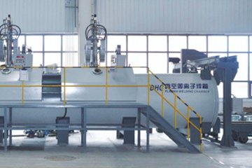
The Ti-Sync™ 4-Stage Refining Protocol: Ensuring Material Integrity
We don't just melt metal. We engineer it. To solve the problem of gas-phase impurities and non-uniform grain structures, we developed the Ti-Sync™ Refining Protocol. This is how we achieve<100ppm oxygen consistently.
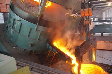
1. Vacuum Induction Melting (VIM)
The process begins in a high-vacuum environment. We strip away volatile impurities and ensure the base chemistry is locked in. This stage focuses on removing Carbon and Nitrogen that can embrittle the target.
2. Electron Beam (EB) Multi-Refining
This is where the magic happens. A high-energy electron beam melts the titanium, allowing ultra-low vapor pressure impurities to evaporate. By cycling this process, we push the purity from 4N to 6N levels. It's slow. It's expensive. It's necessary.
3. Grain Size Stabilization
Sputter yield is a function of crystal orientation. Through proprietary thermomechanical processing, we ensure a fine, equiaxed grain structure (typically < 100μm). This minimizes "nodule" growth during sputtering.
4. Cryogenic Machining
Final shaping occurs under cryogenic cooling. This prevents heat-induced oxidation of the surface and ensures the target arrives at your cleanroom with a pristine, defect-free topography.
Advanced Manufacturing and Quality Control Standards
Trust but verify. Our analytical lab utilizes Glow Discharge Mass Spectrometry (GDMS) to detect trace elements at the parts-per-billion (ppb) level. While ICP-MS is good, GDMS is the gold standard for solid metallic samples because it provides a full-spectrum analysis of every contaminant.
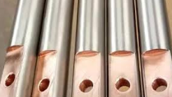
Every target shipped from our facility comes with a certified COA (Certificate of Analysis) mapping the impurity profile. We also use ultrasonic non-destructive testing (NDT) to ensure 100% bonding integrity for targets mounted on OFHC copper backing plates.

Technical Specifications and Sputtering Yield Data
Success in the PVD chamber requires more than just purity. Thermal management is critical. Titanium has a relatively low thermal conductivity compared to copper, making target cooling a priority during high-power runs.
| Property | Value |
|---|---|
| Theoretical Density | 4.506 g/cm³ |
| Melting Point | 1668°C (3034°F) |
| Thermal Conductivity | 21.9 W/(m·K) at 20°C |
| Sputtering Yield (Ar+, 500eV) | ~0.51 atoms/ion |
Frequently Asked Questions
What is the typical lead time for custom 6N titanium targets?
Standard circular targets often ship in 2-3 weeks. Custom geometries or large-format planar targets requiring the full Ti-Sync™ protocol typically range from 4 to 6 weeks depending on the refining cycles required.
How do you handle backing plate bonding for high-power applications?
We utilize metallic bonding (Indium) or diffusion bonding depending on the thermal load. For high-power density processes, diffusion bonding is preferred to prevent target debonding at elevated temperatures.
Why is grain orientation so important for film uniformity?
Titanium has a hexagonal close-packed (HCP) structure. Sputtering rates vary significantly across different crystal planes. If your target has "clumpy" grain orientation, you get uneven film thickness on your wafer. We control this via thermomechanical processing.
Optimize Your PVD Yield Today
Don't let trace impurities compromise your semiconductor performance. Contact our engineering team for a technical consultation on 5N and 6N Titanium specifications.
Request a Quote