


Precision Vacuum Creep Flattening: Achieving Ultra-Flat Titanium
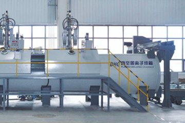
In the high-stakes world of semiconductor manufacturing, "close enough" is a failure. As of 2026, the demand for extreme precision in semiconductor titanium parts has reached a fever pitch. Whether you are designing a 12-inch wafer handling system or an etching chamber, the flatness of your base material dictates the performance of the entire tool. Vacuum Creep Flattening (VCF) has emerged as the gold standard for achieving these impossible tolerances.

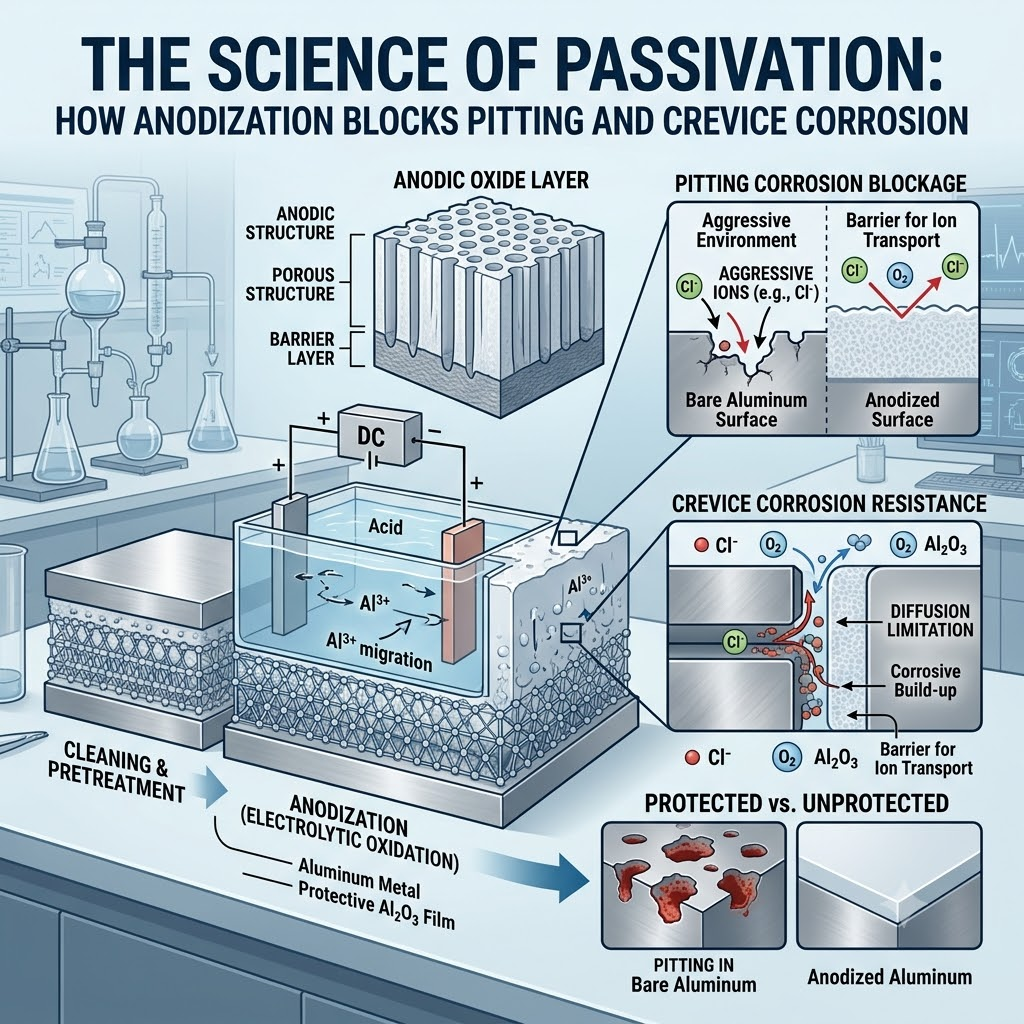
"Vacuum Creep Flattening is a thermal process that utilizes the synergy of atmospheric pressure and high-temperature creep behavior to reshape titanium plates within a vacuum environment, permanently eliminating internal residual stresses."
At China Titanium Factory, we view flatness not as a mechanical suggestion, but as a thermal mandate. Our engineering team defines the Golden Rule of VCF: Flatness is a thermal memory, not a mechanical state. To fix a plate, you must reset its molecular history.
The Physics of Failure: Why Cold Leveling Cannot Meet Semiconductor Demands
Traditional cold leveling—using rollers or presses at room temperature—is the enemy of precision titanium. The reason lies in the material's DNA. Titanium possesses an elastic modulus of approximately 103-116GPa. This is roughly half that of steel. When you bend it cold, it fights back.
This "springback" phenomenon means that even if a plate looks flat after a press, the internal residual stresses are lurking. As soon as you begin CNC machining or expose the part to the thermal cycles of an etching chamber, the plate warps. It "remembers" its original curve.
VCF bypasses this by operating at annealing temperatures. By holding the titanium plates under a vacuum seal, we allow atmospheric pressure to exert a perfectly uniform force across the entire surface. The material "creeps" into a state of zero stress. It doesn't just look flat; it is flat at a molecular level.
Flatness Tolerance Comparison: Standard Commercial vs. Special Precision
For procurement officers and engineers, understanding the delta between commercial standards and semiconductor-grade VCF is critical. According to NIST material standards, standard leveling is often insufficient for vacuum integrity.
| Feature | Standard Commercial | VCF Special Flatness |
|---|---|---|
| Flatness Deviation | 1.0mm per 1000mm | < 0.06 inch / 12 inch (0.01mm-0.05mm) |
| Residual Stress | High (Subject to warping) | Near-Zero (Dimensionally stable) |
| Surface Finish | Roller marks possible | Mirror-like, oxygen-free |
| Process Reliability | Inconsistent | Highly repeatable via PLC control |
The VCF-Alpha Precision Protocol: Our Proprietary 3-Phase Methodology
At China Titanium Factory, we don't just "heat and hope." We utilize the VCF-Alpha Precision Protocol to ensure every plate meets semiconductor etching chamber requirements.
Phase 1: Multi-Zone Thermal Mapping
We use high-fidelity sensors to map the furnace's thermal profile. Uniformity is key. A variance of even 5°C across a large titanium grade 5 plate can lead to uneven creep rates.
Phase 2: Atmospheric Pressure Optimization
By creating a high vacuum (< 10^-3 Pa), we allow the external atmosphere to act as a massive, invisible hydraulic press. This applies tons of perfectly distributed force without the localized "hot spots" of mechanical clamping.
Phase 3: Controlled Cryogenic-Inert Cooling
Rapid cooling reintroduces stress. We utilize a slow, argon-quenched cooling cycle that "locks" the flat grain structure in place. This ensures the plate remains stable during heavy CNC milling.
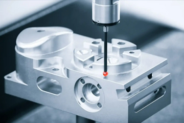
How to Measure Titanium Plate Flatness Using Three-Coordinate Inspection (CMM)
Verification is the final pillar of trust. You cannot measure ± 0.01mm with a straightedge and a feeler gauge. We follow a strict inspection process:
Datum Establishment: The plate is placed on a Grade 00 granite surface plate. We establish a primary plane using a minimum of three points.
Point Cloud Collection: Using a Ruby-tipped CMM probe, we collect a high-density grid of points (e.g., a 50mm x 50mm grid) across the entire surface.
Deviation Mapping: Software calculates the distance between the highest and lowest points relative to the theoretical flat plane.
Stress Testing (Optional): For critical parts, we perform a "vibration stress relief" check to ensure the CMM readings remain consistent after simulated handling.

Critical Applications in Semiconductor Equipment
Why go to this trouble? Because in 2026, the node sizes are smaller than ever. In a semiconductor etching chamber, the plasma must be perfectly uniform. If the titanium electrode or chamber wall is bowed by even 0.05mm, the plasma density shifts. This leads to wafer scrap costs that can reach hundreds of thousands of dollars.
Our VCF-processed plates are found in:
Wafer Handling Equipment: Precision end-effectors that must remain flat to prevent wafer slippage.
Vacuum Chamber Integrity: Large-scale chamber lids that require a perfect vacuum seal against an O-ring.
Etching Plates: Components exposed to corrosive gases where surface integrity and flatness prevent localized pitting.
Procurement and Logistics: Sourcing the Best
Sourcing VCF-treated material requires a partner with the right certifications. Look for Nadcap (National Aerospace and Defense Contractors Accreditation Program) or ISO 9001:2015 at a minimum. These ensure the thermal cycles are calibrated and traceable.
Lead times for custom titanium fabrication involving VCF typically range from 4 to 8 weeks, depending on the plate size and the complexity of the cooling cycle. At China Titanium Factory, we maintain a buffer of pre-flattened stock to support urgent R&D requirements for global semiconductor fabs.
Frequently Asked Questions
Does VCF affect the mechanical properties of Grade 5 titanium?
VCF is performed at temperatures below the beta-transus point. This means it acts as a stress-relief anneal, which generally improves ductility and fatigue resistance without sacrificing the high tensile strength of the alloy.
What is the maximum thickness for Vacuum Creep Flattening?
While we can process plates up to 150mm thick, VCF is most effective for thicknesses between 5mm and 80mm. For extremely thick blocks, thermal soaking times increase significantly to ensure the core reaches the target temperature.
Will the plate stay flat after I machine it?
Yes. This is the primary advantage of VCF. Because the internal residual stresses are removed, removing material during CNC milling will not cause the "potato chip" warping common with cold-leveled plates.
Ready for Semiconductor-Grade Precision?
Stop fighting material springback and start building with confidence. Our VCF-Alpha Precision Protocol delivers the flatness your etching chambers demand.
Get a Technical Consultation Today